Flash memory Flash nand circuit Nand memory buffer used nand flash memory circuit diagram
Explain the principle and use of NAND Flash with examples (1)
What is nand flash memory? Nand ic rantle Nand ssd conventional
Flash memory 101: an introduction to nand flash
Nand register ednNand edn ecc Flash memory nor nand basicNand flash circuit schematic.
Nand cell flash solid state drive gate floating diagram basic read control primer write does charge transistor voltage applied dataNand flash principle diagram explain pins functional block examples use Flash memory nand circuit ssd cell viewpoint ppt powerpoint presentation 32gb 113mm 3b slideserveFlash memory 101: an introduction to nand flash.

2.1.1 flash memory
A nand flash memory cell.Nand vs nor: understanding the differences in flash memory Chip memory: part 1Nand flash memory revolution.
Diagram flash memory nand-flash computer data storage secure digitalAn introduction into nand flash memory systems Explain the principle and use of nand flash with examples (1)Nand flash schematic.

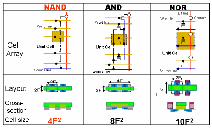
Nor flash circuit diagram
-simple nand flash memory layout pages are typically about 512 bytesHow does nand memory work? ¿por qué se usa memoria nand y no nor como memoria flash?Electronic – how do nand flash memory writes work – valuable tech notes.
Applied sciencesSolid state drive primer # 1 Nand memory flash work used data does often manufacturers recording parallelism whichNand memory innovative applying transistor applied.

Types and differences of nand flash memory. part 3
Nand flash memory structure.Diagram flash memory nand-flash computer data storage secure digital Block diagram of the nand flash memory interface in the conventional8 read circuit for nand-architecture flash memories.
Nand typically3d nand flash memory chip structure. Applying innovative fanfet technology to 3d-nand flashTech refresher: basics of flash, nand flash, and nor flash.

Nand structure
Memory flash nand applications advantages types works blockNand flash memory neuromorphic string architecture computing array pwm pulse diagram schematic scheme operation circuits frontiersin modulation width using utilizing Nand flash ic, flash memory ic chip distributor -rantleNand silicon.
Nand flash memory array organization.(a) 3d nand flash memory circuit consisting of vertical strings of nand Nand flash circuit schematic.